(c) 2000, Bas de Jong PE1JPD
Introduction
This transceiver is designed for high-speed packetradio in the 23cm band using Frequency Shift Keying with baudrates from 9k6 up to 150 kbit/sec depending on the IF-bandwidth and modulationtype.
| A kit or ready made unit is available from DDS Electronics, the Netherlands |
Please read this manual carefully and follow the steps for construction and alignment. In this manual you will find the following chapters:
Specifications
| General | |
| Vcc supply | 12-14 V |
| Frequency range | 1241.000 –
1241.950 1295.000 – 1295.950 other segments possible as option |
| Pullingrange within channel | +/- 25 kHz |
| Modulation | Wide Band FM |
| Receiver | |
| Sensitivity | -100 dBm |
| Noiselevel | ~3.5 dB |
| RxM output | 1V top-top with100 kHz dev. |
| RxD output | 5V top-top |
| RSSI | |
| Squelch status (mute) | Available |
| Transmitter | |
| Power output | 2 – 3 Watts |
| Deviation | ~10 - ~100 kHz or wider |
| RX/TX switchtime | ~10 ms |
| Overheating during TX | Without heatsink ~3
min With heatsink dependent on size of it |
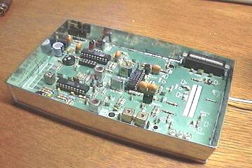
Description
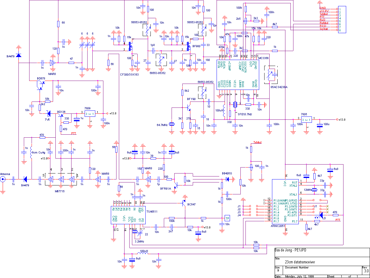
The design of the transceiver is straightforward and shown in fig. 1. Central in the design is the vco which oscillates directly on the transmit-frequency around 1241 or 1295 MHz . The vco is build around a BFR91A with a stripline-filter between collector and basis of which the center stripline can be tuned with a varicap. This vco has a very low noiselevel but the tuningrange is rather limited to around 100 MHz, which however is sufficient for this purpose. The vco is followed by a mar-8 which acts as a buffer/amplifier with an output of 10-15 mW. A small part of this output is fed to the TSA5511 PLL. This IC integrates everything which is needed for the PLL: programmable devider, reference oscillator and devider, phasedetector and amplifier. The device is programmable via I2C. The output-frequency of the vco is determined as follows:
Fvco = Fref * 8 * n where Fref = Fxtal/512
With Fxtal = 3.2 MHz Fvco = n * 50 kHz so the output frequency fits in a 50 kHz raster. The referencefrequency can be pulled a bit with the trimmer in series with the 3.2 MHz crystal.
The PLL is programmed by the microcontroller AT89C2051. This is a member of the 8051-family with serial input/output, 2 parallel ports and a analog comparator. The clockfrequency of the controller is not critical at all and is determined by a crystal (12 MHz). The vco-frequency is controlled via 6 jumpers of which the most significant bit (J5) determines the bandsegment of the vco (1241 resp. 1295 MHz). The other 5 bits determine the frequency in 50 kHz steps:
543210
X00000 1241.000
X00001 1241.050
....
X10011 1241.950
As already stated, the trx is designed to be used split-frequency where the IF equals the split. This way the frequency of the vco doesn't have to be changed during rx or tx, and no time is lost (re)programming the PLL and locking up again. Therefor very fast switching times can be achieved which are needed for high-speed packet. The output from the vco/buffer is fed into a striplinecoupler at the rx-mixer build around a 3SK183 dual-gate mesfet. During rx, the antenne-input is fed via a quarter wavelength stripline to a mar-8 amplifier giving 20 dB gain, followed by a 3 line striplinefilter. This striplinefilter is tuned with sky-trimmers. The output of this filter directly couples to gate-1 of the rx-mixer fet, together with the LO-signal from the vco/buffer. The output of 54 MHz IF is filtered via 2 TOKO-coils, amplified by a BF982 DG mosfet and fed to a MC3356 IF-chain. This IC converts the input to 10.7 MHz using an oscillator build around a BFY90 and a 64.7 MHz crystal. The second IF of 10.7 MHz is filtered in a SFE10.7 IF-filter, amplified and demodulated in a quadrature detector. The demodulated output is available via a feed-through C, as well as a Receive Signal Strength Indicator (RSSI: S-meter), a squelch/mute signal and a shaped, digital output. The IF-bandwidth is determined by the type of filter and is in this case 280 kHz wide.
The tx-path is very straigthforward: via a -20 dB stripline coupler 0.15 mW of the LO-signal is coupled to a third mar-8 giving 20 dB gain. The output of around 10 mW is amplified in a Mitshubishi M67715 module giving 2-3 Watt of output. The tx-modulation from the modem is first filtered via a simple RC-lowpass and then put onto the PLL controlvoltage. The deviation is adjusted via a 100 ohm trimmer. The tx is switched on when PTT is low, which results in switching on of the 9V for the tx mar-8 and the driver-stages in the module. The 9V also supplies the PIN-diodes in the antenna-switch. During tx both diodes conduct so that the output from the module is fed to the antenna, and via the second diode the lambda/4 to the rx-input is transformed to high-Z at the antenna. Finally, the 9V switches off the power for the rx-input mar-8 and the IF-amplified.
Construction
preparation
To build this transceiver you will need the following tools and materials:
Steps
Alignment
Preparation
First check the pcb for shorts, incorrectly placed components (IC's, transistors, regulators, fets). Of course, a programmed Atmel controller should be put in position. Remove all jumpers, this will preset the vco to a frequency of 1241.000 MHz. If it fits better, just put jumper J5 into position so that the output will be 1295.000 MHz.
VCO and PLL
If everything looks ok, power can be applied. Power should be 12-14 V, not more! Now the red LED may give a short flash but should stay OFF indicating that the vco is in lock. Check the vco by putting your (wet) finger on top of the oscilator transistor BFR91A so that the LED turnes on. During the first moments, check whether nothing gets overheated and check the output of the 5V regulator. If possible, check the vco output on a spectrum analyser or 23cm transceiver tuned to 1241 MHz.
The vco is now running on the correct frequency. Try fitting and removing jumper J5; everytime the PLL is reprogrammed and the vco swings from high to low and vv which causes the red LED to give a short flash. If it stays on, the PLL is not in lock. If this only happens either with or without J5, the PLL is ok but fails to lock at one frequency.
Transmitter
Now connect an appropriate powermeter and dummyload to the antennaconnector and ground PTT: 2-3 W should now be available. No tuning is nessecary for the poweramplifier. Only the deviation has to be set using the variable R of 100 ohm. Preset this R halfway. Final adjustment can be done using the modem later on, but in general the modulationlevel is also adjustable on the modem.
Receiver
To align the receiver a 54 MHz signalsource for the second IF is needed. If not available, you can use a 23cm signal on 1241.x or 1295.x MHz, or as a last resort, a 70cm handheld capable of transmitting on 431-433 MHz listening at the third harmonics on 1295.x. Be sure to math the frequencies on 70 and on the transceiver.
Preset the 3 skytrimmers to minimum and the IF coils so that the ferrite dips 1.5 mm in the coil.
Now, get the 64.7 MHz crystaloscillator running first. The output from this oscillator can be monitored with an ordinary scanner or 6m receiver whichever is available. Carefully tune the coil located near the 64.7 MHz crystal until the oscillator fires up. Turn the ferrite anticlockwise until the oscillator turns off again; the maximum output can be achieved just before this happens.
To tune the IF, connect an oscilloscope to the RSSI and apply a signal of 54 MHz -50 dBm to the antenna-input. Tune the IF coils to maximum, and take care to switch off the signal now and then so that output diminishes.
Now connect the oscilloscope to the RxM and tune the quadrature detectorcoil. The 54 MHz signal has to be frequency-modulated with a deviation of 100 kHz. Remove the 54 MHz signal and apply a 23cm signal –50 dBm of the appropriate frequency to the antenna-input and tune the 23cm bandpass. Optimize the IF-coils and the 23cm filter. A sensitivity of –100 dBm should easily be achievable.
tips and backgrounds
Other bandsegments
The transceiver is designed for splitfrequency use around the lower end of the 23cm band at 1241 MHz and 1295 MHz. The IF-shift is therefore 54 MHz. However, it is possible to use other shifts in the range 40-70 MHz. The 64.7 MHz crystal has to be changed accordingly:
F2xtal = IF-shift + 10.7 MHz.
In particular is it possible to use the trx as a linktransceiver in the segments 1240.x and 1299.x by changing the crystal to 69.7 MHz. Since the IF increases from 54 to 59 MHz the inductors in the first IF have to be tuned higher.
Changing the IF-bandwidth
When to be used in the interlink segment, the maximum aloowed bandwidth is 50 kHz. It is appropriate to adjust the second IF-filter accordingly. The filter used, a SFE10.7MA is 280 kHz wide but there are also filters available which are narrower with 30-50 kHz minimum.
Modulation lowpass
Standard a first order lowpass of 1 kohm/1nF is fit on the pcb. It is advisory to change this lowpass to one that fits the maximum modulation frequency.
Modulationtype and bandwidth
This transceiver uses direct FSK for modulation. It can not be used for standard, narrowband 9k6. When using WBFM however, it can be used with manchester FSK from 9k6 - ~115k2 or G3RUH-type modulation from 38k4 - ~200 kbit. Remember that the bandwidth will be
B = 2 * Fmod + 2 * Fdev
Where B is the bandwidth, Fmod is the maximum modulation frequency and Fdev is the deviation used. Fmod for G3RUH equals half the bitrate (4800 Hz for 9k6) or, for manchester, the bitrate. So, when using 38400 baud manchester, the bandwidth will be around 150 kHz.
Working simplex
In principle it is possible to work simplex with this trx. Simplex means that the rx and tx frequencies are the same. When changing from rx to tx or vice versa, the PLL now has to be reprogrammed by the microcontroller. The hardware is prepared for this (the PTT signal is available to the controller at pin 11), but the current version of the software does not support it. Remember that the rx/tx switchingtime will increase significantly because not only time is needed for the PLL to get into lock again, but also the time to reprogram the PLL has to be accounted for.